Single Photons Go for Gold
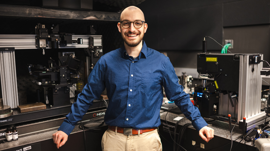
Emanuil Yanev talks about his PhD work modifying 2D materials to push their light-producing limits.

Learn More
In 2015, a class of two-dimensional materials called the transition metal dichalcogenides (TMDs) entered the scientific limelight for their ability to produce just one particle of light at a time. Such single-photon emission was a natural, and somewhat random, ability in TMDs with structural defects—missing atoms here and there, or a wrinkle where the crystal should have been straight and even.
Researchers quickly moved from observing single photon emission in TMDs to attempting to engineer the materials in a way that could yield the same effect on demand. Writing recently in Nature Communications, a team including mechanical engineers Jim Schuck and Jim Hone and the Borys lab at Montana State University go for gold to create a single photon emitter.
They carefully placed atomically thin layers of a TMD called tungsten diselenide (WSe2) on the tips of nanoscopic gold cones, which create tiny wrinkles in the material. Those wrinkles yielded strong evidence of single photon emission that, notably, occurred at room rather than ultracold temperature.
Leading the effort to research the properties of tungsten diselenide is Columbia Engineering PhD student Emanuil Yanev. In this Q&A, Yanev shares what’s so interesting about single photon emitters, his journey from Idaho to New York City, and a little more about himself and his time at Columbia.
Why do we need single photons?
We’ve all heard lots about quantum computers lately, but, eventually, we’ll want to build a network of them—essentially, a quantum internet. Single photons can be really important elements in transferring information while preserving its quantum nature.
How did you come up with the idea of using gold cones for this research?
We’ve been experimenting with using strain to create single photons.
Learn More
In a prior paper published in Nature Nanotechnology, we created “nanobubbles” that strained tungsten diselenide and caused localized photon emission, but we realized that the light was coming from very small wrinkles around the bubble perimeters and not the bubble centers. We thought an array of cones could create similar wrinkles, but in a more robust and prescriptive fashion so we could better determine exactly where the strain originated and where the photons were coming from. Making the cones out of a metal like gold can also enhance the output, like an antenna.
Can we definitively say you can create single photons at room temperature?
Almost. The definitive proof is a correlation measurement that demonstrates antibunching, where you statistically show that there’s zero chance that two photons were emitted at the same time. We’re working on that, but it’s technically challenging with our nano-optical approach.

What we did show was power saturation, which is pretty strong evidence for single photon emission. We excite the tungsten diselenide by shining a laser onto a cone-induced nano-wrinkle. A single photon emitter can’t absorb a second photon until it emits what it has already absorbed from the laser, which takes some time. That means you hit a point where it can’t keep up with the rate of incoming photons, and so the emission output no longer scales with the laser input.
We observed that saturation behavior in our engineered samples at room temperature. This is exciting because it shows that single photons are potentially being created without expensive cryogenic equipment, which so far has been necessary for achieving single-photon emission in TMDs.
What’s next for this research?
To demonstrate antibunching, we need to boost the brightness of the single photon emission, so we’re experimenting with different combinations of materials. We are also starting to think about optimizing the design so that, one day, we can integrate these single photon sources onto circuit chips—that’s the ultimate goal.
Bigger picture, we also want to fundamentally understand what’s going on in these materials. The reason we have smartphones today is because 70-plus years of effort have gone into developing our understanding of silicon—the material that all of our electronics are made from. We’ve pushed the scaling of that technology to the limit more or less, so it’s time to see what we can do with new materials.
And what’s next for you?
I’m nearing the end of my PhD, so I’m starting to write up my thesis. And look for jobs. I’d like to pivot into the quantum computing industry. That’s an exciting space right now. I’ve spent a lot of time doing nanofabrication and working in cleanrooms to make substrates and samples with these 2D materials, and I’d love to continue applying that skillset going forward.
What was your path to your PhD?
My family moved to the US from Bulgaria when I was five, and we ended up in Idaho. Idaho was a great place to grow up, but it’s a little sleepy and I wanted to get into a bigger city, so I enrolled in Columbia’s 3-2 Combined Plan Program. I spent three years at The College of Idaho studying math and physics, then transferred to Columbia to study engineering for another two years.
I've been an engineer at heart since I was young. I always enjoyed tinkering and building random things in our garage. When I got to Columbia, I was really excited by the research efforts directed at the nano-scale. I started working in Jim Hone’s lab, and I decided to stay to pursue a PhD, which has been co-advised by Jim Hone and Jim Schuck.
How has your time been at Columbia?
With Jim Hone, I learned a lot about nanofabrication, 2D material synthesis, and sample preparation, and with Jim Schuck, I learned more about optical characterization and applications of these materials. I was a bit of a bridge between the two labs initially, which was a great opportunity: Jim Schuck had just arrived at Columbia when I started my PhD, so I helped teach a lot of the group how to make samples with 2D materials that we would then study optically.
I also spent time at Brookhaven National Laboratory as a Department of Energy Office of Science Graduate Student Research Fellow, where I had the chance to explore advanced nanofabrication techniques, such as cryogenic plasma etching.
The 2D materials field is a highly collaborative environment, and it’s been really rewarding to work with people from lots of different backgrounds. You have this great overlap of researchers from mechanical engineering, electrical engineering, materials science, chemistry, and physics coming together to tackle problems.
How do you keep busy outside of the lab?

Mountain biking, which is usually not the first thing that comes to mind when you think of Manhattan! I’m on the board of the New York City Mountain Bike Association, which is a nonprofit that builds and maintains the majority of off-road trails in the city and offers free bike clinics for kids and adults.
Almost everyone had a bike where I grew up, but that’s not the case here. We give New Yorkers who wouldn’t otherwise have the opportunity to ride a chance to do so, while also improving the parks for hikers and the broader community.
Any words of advice?
Don’t be afraid to fail. A lot of people coming into graduate school are high-achieving individuals, but research is very different from the classroom—you’re going to be failing a lot, and you can’t internalize that. Just because your experiment was unsuccessful doesn’t mean you are a failure: it’s just part of the process. In fact, some of the greatest insights and discoveries are had when things don’t go according to plan, so keep an open mind!