Columbia Nano Initiative Joins Industry with Academia in Columbia’s Laboratories
In one of her first jobs, Nava Ariel-Sternberg worked in a laboratory at the forefront of nanotechnology research, the study of infinitesimally structures and material. Then, a few years into her career, she realized the life of a bench scientist wasn’t for her. “I wanted to do something practical, interacting with a variety of people but not stray too far from my training,” Ariel-Sternberg said.
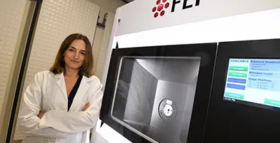
She found the ideal mix at Columbia, which recruited her in 2015 as the inaugural director of shared laboratory facilities, an integral part of the university’s Columbia Nano Initiative(CNI), launched the prior year to support multidisciplinary research.
Ariel-Sternberg, who holds a master’s degree from Technion–Israel Institute of Technology and Ph.D. from the Massachusetts Institute of Technology, oversees 9,000 square feet of lab space in three buildings on the Morningside campus. The state-of-the art facilities bring together more than 100 research groups—engineers, physicists, mathematicians, chemists and data analysts from academia and industry—who collaborate on new materials, methods and procedures to propel the promise of nanotechnology into the world.
Q: Why study nanoscience ? What are the challenges of the research?
A: The ability to image and control individual atoms and molecules has opened up many new possibilities and revolutionized science, and the applications of nanotechnology are endless: in medicine, new and accurate diagnostics and targeted and personalized drug delivery; in neuroscience, noninvasive brain imaging devices; and in materials sciences engineering, new materials and super atoms with tailored structures and properties as well as novel, high-performance devices. With these opportunities, however, come great challenges. We are experimenting with materials invisible to the naked eye and fabricating devices or films too tiny to hold directly. Working with nanotechnology also requires tightly controlled environmental conditions; a fine human hair, for example, is about 1,000 times bigger than a typical nano-device. Nanofabrication research is confined to a clean room lab with filtered air, and researchers wear special apparel and work with equipment that allows for a high level of accuracy and control. Every little mistake can be detrimental when dealing with such small dimensions.
Q. How many labs are in the CNI shared facilities?
A: The CNI Shared Facilities consist of three laboratories: clean nanofabrication lab (5000 sq. ft.); materials characterization lab (2500 sq. ft. ), established and partially funded by the National Science Foundation); and a 1500-square foot electron microscopy lab. Columbia University researchers can obtain access to more than 60 pieces of cutting-edge equipment spread across the labs, which are managed and operated by a specialized technical staff to maintain the equipment, assist users and provide training and guidance.
Q: Are the laboratories open to scientists outside the University?
A: Dozens of research groups use our labs, including scientists from other academic institutions and industrial companies. A few startup companies also use our clean room as their prototyping research lab. One of them is DrinkSavvy, a Brooklyn-based business that developed a nanophotonic platform to detect date rape drugs and is now investigating other applications for that platform. Companies such as Intel turn to us for projects involving specialized techniques, enhancing the collaboration between industry and academia. These companies are able to perform their initial R&D work in an incubation-like environment without having to purchase instrumentation or spend seed money on lab construction. Often, students working in our labs are hired by these companies when they graduate.
Q: How are the labs financed?
A: Nanotechnology research involves significant cost: equipment maintenance, machine parts, materials, air-conditioning and humidity systems, safety systems, gases, chemicals and more. All this is in addition to personnel salaries. The labs operate under licenses provided by the University’s controller and charge nominal user fees to recover some expenses. Industrial users pay three times the internal rate based on the expenses associated with their equipment needs, and outside academic institutions pay similar rates to Columbia users, plus an administrative processing fee. External user fees represent about 20 percent of labs’ operating budget. The remainder comes from the School of Engineering and the Faculty of Arts and Sciences. But the purpose of the program is not to make a profit. The goal is for the nanotechnology community at Columbia and its collaborators to have the proper research infrastructure for the top-notch science they do.
Q: Tell us about yourself. Why did you become an engineer and materials scientist?
A: I was born and raised in Israel, went to graduate school in Boston, Mass., and now I live in New Jersey with my husband and three kids (10, 8 and 5 years old). I always had a passion for science, but as a practical and application-oriented person, I was drawn to the engineering side of field. After obtaining my Ph.D. at MIT, I spent six years working in the semiconductor industry, but I’ve always had a special place in my heart for academia. I love my job. It’s a privilege to lead a professional staff responsible for the unique research infrastructure of CNI and provide researchers with everything they need for the incredible nano science that happens at Columbia.