Jacob Trevino Is Thinking Big About Nanoscience
The director of the Columbia Nano Initiative’s Shared Labs discusses growing nanoscience at the University—and beyond.
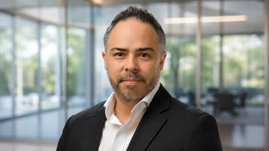
Last year, Jacob Trevino took the helm of the Columbia Nano Initiative’s (CNI) Shared Laboratories. These include a state-of-the-art nanofabrication cleanroom, a lab with specialized instruments to determine the properties of different materials, and an electron microscopy lab, all available to Columbia researchers as well as academic and industry partners around the city who are pushing the limits of nanoscience.
Trevino has watched this “small” science grow over the last 25 years, since his first foray into the field as a summer Research Experiences for Undergraduates (REU) student at Pennsylvania State University. “At the time, nanotechnology was still emerging, but you could already see that it had the potential to impact nearly every area of technology,” he recalled. “I wanted to be a part of it.”
Throughout his career, Trevino has worked on microelectromechanical systems (MEMS) for NASA; contributed to the development of inertial accelerometers now found in everything from aircraft to Nintendo Wii controllers; and published extensively on nanophotonics for solar energy, sensing, LED technologies, and quantum devices. He also co-founded Chemeleon, a startup focused on point-of-need chemical and biological diagnostics.
Trevino has also helped build and expand academic nanofabrication facilities across the East Coast and, in 2018, founded NanoTech NYC, a nonprofit dedicated to strengthening and connecting the nanotechnology community throughout the New York metropolitan region.
As CNI Labs senior director, Trevino is still thinking big about nanoscience and growing Columbia’s “nanofab” role in the city—and beyond.
What brought you to Columbia and CNI?
In 2013, I was the founding director of the City University of New York’s (CUNY) Advanced Research Science Center (ASRC) Nanofabrication Facility, which we built from scratch. I had to figure out who the nanoscience community in the area was and what their needs were. I started mapping the people, resources, and challenges in the region and then set out to build connections among universities, including CUNY, New York University (NYU), Columbia, and others. Eventually, I was recruited to NYU Tandon to help stand up their new Nanofabrication Cleanroom, before moving to the University of Pennsylvania to continue their nanofab initiatives at the Singh Center for Nanotechnology.
When Nava Ariel-Sternberg decided to leave CNI for a position at ASML, Professor Michal Lipson reached out to me. Columbia already felt familiar. Over the years, I had helped establish collaborative agreements between the ASRC and CNI, and I had been teaching Principles of Device Microfabrication at Columbia since 2015. I also knew that Nava and the CNI team had built an outstanding facility with a strong staff and culture. Combined with the University’s clear commitment to supporting and growing CNI, the decision to join was very easy.
What are your priorities?
Nava led the major renovation that transformed CNI into the facility it is today. Our focus now is on elevating its national profile by expanding engagement with external researchers from established companies to startups, and building stronger partnerships among regional nanofabrication facilities with complementary capabilities.
A key step in that direction has been the launch of NEMO, a new lab management platform that we rolled out in April. Beyond managing CNI’s instrumentation and user operations, it increases the visibility of our facilities to the broader research community. Researchers at other universities can quickly discover what capabilities exist at Columbia, making it easier to identify opportunities for collaboration.
We are also getting ready to launch FabuBlox, a design and process management platform to model and share process flows. It will improve collaboration and knowledge sharing within CNI, and continue to expand our visibility beyond Columbia.
How has nanoscience changed in the past 25 years?
One of the most exciting changes has been seeing nanotechnology move from the research lab into everyday products. Think of your smartphone. Every component—the screen, the cameras, microphones, the sensors—contains elements that depend on nanofabrication techniques.
At the same time, our fabrication tools have become so sophisticated that we’re now working at near-atomic scales and beginning to harness quantum effects in practical devices. It’s an exciting time because we’re seeing the next wave of technologies move from the lab into the real world.
How does a place like CNI help push quantum science forward?
At this stage, quantum is really a materials challenge. In the past, much of the focus was on device fabrication itself, but today, breakthroughs often come from the materials that enable quantum behavior. Right now, much of the expertise and materials still live within individual research groups. One of the biggest challenges is bringing those capabilities into shared user facilities so they become accessible to a broader community.
That means we need to develop staff with materials science expertise and experience, and to offer quantum-ready process flows that are accessible on our tools. Quantum has more factors to consider than our existing processes, and there isn’t just one quantum path: there are photonics, superconductors, 2D materials … each with different needs and requirements.
How are you thinking about building connections in the larger nanoscience ecosystem?
A large part of my role is connecting researchers with the resources they need—whether that’s capabilities within CNI, specialized vendors, or collaborators at national laboratories and other universities.
I’ve been fortunate to work at nanofabrication facilities across the country, which has helped me build a broad network. New York City has an incredible concentration of nanotechnology talent—research institutions, startups, and industry—but many of these groups still operate in silos. That’s one of the main reasons I founded Nanotech NYC to help build connections and strengthen collaboration across the ecosystem.
Looking forward, I think it’s equally important to strengthen the link between New York City and upstate New York. The city has tremendous strengths in research, entrepreneurship, and startup development, while upstate has the infrastructure needed to scale manufacturing. Connecting those pieces will be critical as emerging fields like photonics and quantum continue to grow.
What has been the most remarkable effort you’ve seen come out of CNI labs since you took over?
I’ve always admired the work from Cory Dean’s physics lab. In recent years, they’ve published a number of groundbreaking studies on transition metal dichalcogenides, especially WSe₂, pushing the boundaries of both quantum materials research and device fabrication.
What do you do when you need a break from nano?
Outside of work, I enjoy snowboarding in the winter and golfing in the warmer months. Snowboarding is a great way for me to disconnect and recharge, while golf keeps me humble. I’m not very good at it, but I love the challenge.