Nanoscience 101: A Q&A With the Engineering School's Jim Yardley
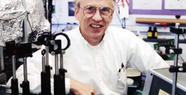
Jim Yardley has seen firsthand how the nanotechnology field has exploded over the past decade. “It’s extremely exciting,” says the managing director of Columbia’s Nanoscale Science and Engineering Center. “The work here has helped create a whole new world of research, a completely new field.” The nanotechnology projects Yardley oversees bring together faculty and students from a host of different departments, including chemistry, engineering, biology and physics, to broaden and deepen our understanding of materials at the molecular level. A chemist by training, Yardley was previously a professor at the University of Illinois and came to Columbia in 2000 after more than 25 years in industry, including stints at Honeywell and AlliedSignal.
Q. What is nanotechnology?
First, you have to know that nano means one-billionth. Then you should know that 1 meter is a scientist’s standard distance. So a nanometer is a billionth of a meter. How do you put that in context? Well, engineers have learned to make smaller and smaller chips. Remember microprocessing? Micro is a millionth of a meter. Today we make chips at 22 nanometers.
Q. Why is nanotechnology important?
Nanotechnology allows you to go in with little hands—not your own hands but nanotechnology’s hands—and do things that would be impossible otherwise. There are three areas of people’s lives that nanotechnology will affect in very visible, measurable ways in the near term. Medicine, computers and mechanics—materials, physical things.
Q. Can you describe the way it works?
In medicine, for instance, you can take a pill and (the cancer-fighting agents) go around your body until they find a cancerous cell and they recognize it’s a cancerous cell and they kill all the nasty cancerous activities, leaving everything else alone. And that is happening right now. There’s also a revolution in the ability to analyze or diagnose disease, built on DNA sequencing. The nanotechnology lets you go in and measure the DNA sequences and find out precisely what they do. Another area is electronics. We all know that computers get faster and cheaper every year. But you may have noticed that in fact that process has slowed down; it’s not happening quite as fast as it was five years ago, and there’s a reason. There are physical limitations to what you can do with silicon semiconductor technology. Nanotechnology, in principle, can let you go way beyond that to continue to build electronic devices that are more powerful, cheaper, faster and use less power—all good things.
Q. Explain how the technology affects materials.
Consider graphene, a material we pioneered at Columbia and one of the strongest materials known to man. In principle you could build physical objects out of this stuff that would be stronger, lighter and much more useful. But it’ll take a long time before ordinary people see the results of nano in mechanics, in spite of those ads you may have seen for golf clubs or tennis racquets that have carbon nanotubes in them.
Q. Is nanotechnology still in the basic research phase, or are there already applications?
When the National Nanotechnology Initiative was started in 2000, its founders laid out a road map for nanotechnological development. First came very simple applications such as improved sunscreens—nanoparticles that would absorb light better on your body—and improved golf clubs. When you really dig down, they’re relatively trivial applications. Nanotechnology applications are out there today, but they’re not affecting people’s lives today in the same way that they will 10 years from now.
Q. Why is research on the nanoscale so different from the way scientific research has traditionally been done?
The complexities of nanoscience require disciplines to work together. So research in nanotechnology almost by definition is multidisciplinary. When we created the Nanoscale Science and Engineering Center here at Columbia in 2001, we brought together a set of chemists, physicists and engineers. They all worked together and learned to speak the same language so they could do the things you have to do to build and understand things on the nanoscale. Some people ask whether nanotechnology should be its own discipline. Here at Columbia we think by and large that it’s much better to have conventional disciplines with great depth and then pull together special groups or teams for the end result.
Q. What is the Columbia Nanoscale Science and Engineering Center?
Columbia started the center in 2001. It was given a 10-year commission by the National Science Foundation, with a significant level of funding to support the research of about 20 professors and their graduate students. Our program was called the Center for Electron Transport in Nanoscale Systems, and our mission was to understand the fundamentals of how electrical charges move in systems that are nanoscale. We know the rules about how electronic charges move in macroscopic objects and also in atoms, but we don’t know the rules about how they move in various nanoscale systems. In our center we elected to work on three different systems. One of the systems is carbon nanotubes, which are little tubes of carbon atoms rolled in a funny hexagonal structure. We’ve grown them here to be several meters long, but they typically are only 1 or 2 nanometers in diameter. This structure has electrons that move freely along that tube. So the issue is: How do those electrons move and how can I control them? It’s very different from how they move through a copper or a silicon semiconductor. And so, working partly in collaboration with colleagues at IBM, we have developed a deep understanding of how charges move in carbon nanotubes, which has allowed IBM to develop electronic devices that are built on carbon nanotubes. You can get an awful lot of those on a substrate or a chip. Our nanocenter has also pioneered research in graphene—a sheet of carbon atoms in a hexagonal structure which is only a single atom thick. Finally, we have made major advances in the understanding of how electric charge moves through single molecules!
Q. The center opened 10 years ago. Is that old in the nanoscale world—and what happens next?
All our experiments have created new opportunities. We have a whole set of new programs exploring the electronics, mechanics and biological implications of graphene. It’s like a flat version of a carbon nanotube. Another program is the Energy Frontier Research Center, where the idea is to take everything we’ve learned about how electrons move through nanoscale systems and apply it to photovoltaic devices, where we’ve long known that the key dimensions are a few nanometers. If I don’t grab the electrical current on a distance of a few nanometers, it gets lost. And so by structuring and building such devices on a nanometer scale, we can actually extract charges—electric current—from photovoltaic cells much better.
Q. What different fields need to come together to explore nanotechnology, and what is the scale they need to operate on?
One of the fundamental issues relating to nanotechnology is how do the mechanical properties change when things are small. Suppose I’ve got a block of some material here and I make it smaller; certain properties stay the same—for example, the color of the material. But when it gets down to the nanoscale, that isn’t true anymore. To continue the example, the color of a material on the nanoscale changes with its size. It isn’t just an issue of the mechanics; it’s an issue of where the electrons are and what they do. Who’s going to answer that question in the kind of depth that you need? The answer is, you’d better go to a physicist if you want to understand the electrons and what they’re doing in this process. If you ask the question, “How do these materials interact with themselves and the world?” you’d better have a chemist who can tell you. So you really need chemistry, engineering and physics to understand in depth how to determine the mechanical properties of a nanoscale object. The same sort of thing holds for properties of electronic devices. Electrical engineers should know, right? But there are some strange things that happen with electrons in the nanoscale, and it would not be a normal part of the electrical engineer’s training to fully understand them. He or she really needs to work with a physicist who delves deeply into the nature of electron motion. And you can’t make these things without the chemists. That’s why you need to bring these people together—so they walk into the same labs and look over each other’s shoulders. They work together, they talk about the problem, they learn to express the nature of that problem together.
Q. What effect has nanoscale research had on Columbia as a whole?
When I came here 12 years ago and I walked up and down the halls, you’d hardly see anybody. But now when you walk up and down the halls, you see people arguing with each other, holding samples, animated in discussion. This idea of interdisciplinary research, how you can get more than the sum of the parts by bringing together physicists, engineers and chemists to do collaborative research, was really pioneered here at Columbia. Columbia is one of the key leaders in the university community in nanotechnology, and that really has come about because of the collaborative environment that has been created here. Now we are recognized worldwide as one of the leaders in the development of nanotechnology, especially at the fundamental level. We have truly created the fundamental understanding of charge movement in molecules. We have created the fundamental understanding of graphene, what it is and how it works. We have created fundamental knowledge about carbon nanotubes. And while those have all fostered research throughout the world, the leadership is still here. And I think it’s widely recognized as such.